- 您现在的位置:买卖IC网 > Sheet目录318 > CAT9532WI-T1 (ON Semiconductor)IC LED DRIVER LINEAR 24-SOIC
CAT9532
The Input Register 0 and Input Register 1 reflect the incoming logic levels of the I/O pins, regardless of whether the pin is
defined as an input or an output. These registers are read only ports. Writes to the input registers will be acknowledged but will
have no effect.
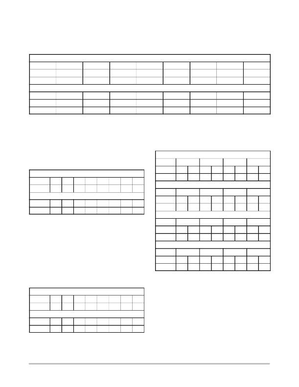
Table 7. INPUT REGISTER 0 AND INPUT REGISTER 1
INPUT0
LED 7
LED 6
LED 5
LED 4
LED 3
LED 2
LED 1
LED 0
bit
default
7
X
6
X
5
X
4
X
3
X
2
X
1
X
0
X
INPUT1
LED 15
LED 14
LED 13
LED 12
LED 11
LED 10
LED 9
LED 8
bit
default
7
X
6
X
5
X
4
X
3
X
2
X
1
X
0
X
The Frequency Prescaler 0 and Frequency Prescaler 1
registers (PSC0, PSC1) are used to program the period of the
pulse width modulated signals BLINK0 and BLINK1
respectively:
T_BLINK0 = (PSC0 + 1) / 152;
T_BLINK1 = (PSC1 + 1) / 152
Every LED driver output can be programmed to one of
four states, LED OFF, LED ON, LED blinks at BLINK0 rate
and LED blinks at BLINK1 rate using the LED Selector
Registers (Table 10).
Table 10. LED SELECTOR REGISTERS
LS0
Table 8. FREQUENCY PRESCALER 0 AND
FREQUENCY PRESCALER 1 REGISTERS
PSC0
bit 7 6 5 4 3 2 1 0
default 0 0 0 0 0 0 0 0
PSC1
bit 7 6 5 4 3 2 1 0
default 0 0 0 0 0 0 0 0
The PWM Register 0 and PWM Register 1 (PWM0,
PWM1) are used to program the duty cycle of BLINK0 and
BLINK1 respectively:
bit
default
LS1
bit
default
LS2
bit
LED 3
7 6
0 0
LED 7
7 6
0 0
LED 11
7 6
LED 2
5 4
0 0
LED 6
5 4
0 0
LED 10
5 4
LED 1
3 2
0 0
LED 5
3 2
0 0
LED 9
3 2
LED 0
1 0
0 0
LED 4
1 0
0 0
LED 8
1 0
Duty Cycle_BLINK0 = PWM0 / 256;
default
0
0
0
0
0
0
0
0
Duty Cycle_BLINK1 = PWM1 / 256
LS3
After writing to the PWM0/1 register an 8 ? bit internal
counter starts to count from 0 to 255. The outputs are low (LED
on) when the counter value is less than the value programmed
into PWM register. The LED is off when the counter value is
bit
default
LED 15
7 6
0 0
LED 14
5 4
0 0
LED 13
3 2
0 0
LED 12
1 0
0 0
higher than the value written into PWM register.
The LED output (LED0 to LED15) is set by the 2 bits
Table 9. PWM REGISTER 0 AND PWM REGISTER 1
PWM0
bit 7 6 5 4 3 2 1
0
value from the corresponding LSx Register (x = 0 to 3):
00 = LED Output set Hi ? Z (LED Off – Default)
01 = LED Output set LOW (LED On)
10 = LED Output blinks at BLINK0 Rate
default
1
0
0
0
0
0
0
0
11 = LED Output blinks at BLINK1 Rate
PWM1
bit
default
7
1
6
0
5
0
4
0
3
0
2
0
1
0
0
0
http://onsemi.com
8
发布紧急采购,3分钟左右您将得到回复。
相关PDF资料
CAT9552HV6I-TG2
IC LED DRIVER LINEAR 24-TQFN
CAV24C02YE-GT3
IC EEPROM I2C SRL 2KB 8TSSOP
CAV24C04YE-GT3
IC EEPROM 4KB I2C SER 8TSSOP
CAV24C08YE-GT3
IC EEPROM I2C SRL 8KB 8TSSOP
CAV24C16YE-GT3
IC EEPROM I2C SRL 16KB 8TSSOP
CAV24C32YE-GT3
IC EEPROM I2C SRL 32KB 8TSSOP
CAV24C64YE-GT3
IC EEPROM I2C SRL 64KB 8TSSOP
CAV4201TD-GT3
IC LED DVR 350MA STP-DN TSOT23-5
相关代理商/技术参数
CAT9532WI-T1
制造商:ON Semiconductor 功能描述:IC PROGRAMMABLE LED DIMMER SOIC-24
CAT9532WI-T1-CUT TAPE
制造商:ON 功能描述:CAT9532 Series 25 mA 5.5 V 400 kHz I2C 16-bit Programmable LED Dimmer - SOIC-24
CAT9532YI
功能描述:LED照明驱动器 16-Bit Prog LED Dimmer w/Interface RoHS:否 制造商:STMicroelectronics 输入电压:11.5 V to 23 V 工作频率: 最大电源电流:1.7 mA 输出电流: 最大工作温度: 安装风格:SMD/SMT 封装 / 箱体:SO-16N
CAT9532YI-T2
功能描述:LED照明驱动器 I2C/SMBus Expander w/LED Dimming RoHS:否 制造商:STMicroelectronics 输入电压:11.5 V to 23 V 工作频率: 最大电源电流:1.7 mA 输出电流: 最大工作温度: 安装风格:SMD/SMT 封装 / 箱体:SO-16N
CAT9534HV4I-G
制造商:Rochester Electronics LLC 功能描述: 制造商:Catalyst Semiconductor 功能描述:
CAT9534HV4I-GT2
功能描述:接口-I/O扩展器 8-BIT I2C/SMBUS I/O PORT RoHS:否 制造商:NXP Semiconductors 逻辑系列: 输入/输出端数量: 最大工作频率:100 kHz 工作电源电压:1.65 V to 5.5 V 工作温度范围:- 40 C to + 85 C 安装风格:SMD/SMT 封装 / 箱体:HVQFN-16 封装:Reel
CAT9534HV4I-GT2-CUT TAPE
制造商:ON 功能描述:CAT9534 Series 2.3 to 5.5 V 8-bit 8 I/O I? and SMBus I/O Port - TQFN-16
CAT9534WI-GT2
功能描述:接口-I/O扩展器 8B I2C &SMBus I/O PORT RoHS:否 制造商:NXP Semiconductors 逻辑系列: 输入/输出端数量: 最大工作频率:100 kHz 工作电源电压:1.65 V to 5.5 V 工作温度范围:- 40 C to + 85 C 安装风格:SMD/SMT 封装 / 箱体:HVQFN-16 封装:Reel
